Disconnections
Admissible linear defects in a crystal
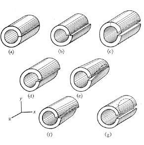
Defects in a crystal can be built using the Volterra process as shown below, in the framework of a continuous media. Consider an elastic solid cut onto a surface bonded but the curve. Every points in the adjacent parts of the cut is moved by a proper symmetry operation W corresponding to:
-
Translation W(I,t) leading to dislocations (b) to (d)
-
Rotation W(R,0) leading to disclinations (e) to (g) 4

Dislocations, contrary to disclinations, are common objects in metals. However, they can be described similarly by considering that dislocations are disclination dipoles, or that disclinations result from dislocation walls.
Interfacial defects and bicrystallography
Interfacial defects are known to play important role in phase transformation, especially in diffusionless ones such as martensitic transformations or twinning. The literature on this topic has adopted different terminology to characterize such defects, focusing either on their step character (growth and structural ledges) or on the dislocation character (transformation dislocations in twinning).
The term of disconnection was coined by J. P. Hirth 1, following the work of R. C. Pond reviewed in a seminal paper 2. It can be defined as an interfacial line defect 3 with both a dislocation and step character.
The concept of step associated with dislocation can be first easily understood by considering a lattice dislocation emerging at a free surface. The step formed results from the inclination of the interface normal with respect to the Burgers vector of the incoming dislocation.

The admissible defects that separates two crystallography equivalent crystals can be determined rigorously. They depend how the two crystals can be connected along an interface . As for defects in single crystal, they can be constructed through a Volterra process considering a bicrystal. However, contrary to the single crystal case, the diversity of interfacial defects arises from the combination of symmetry operations of the two adjacent crystals.
Consider two crystals \lambda and \mu that can be transformed one into the other by a transformation {\bf P}=(P,\vec{p}), P being a lattice rotation/deformation and \vec{p} is the origin shift . The two lattices admit symmetry operations, namely, {\bf W(\lambda)}=(W(\lambda),\vec{w}(\lambda)) and {\bf W(\mu)}=(W(\mu),\vec{w}(\mu))

One class of interfacial defect can then be constructed considering that the breaking symmetry introduced is a translation, i.e. {\bf W(\lambda)}=(I,\vec{t}(\lambda)) {\bf W(\mu)}=(I,\vec{t}(\mu)) or expressed in the \lambda lattice {\bf W^\ast(\mu)}=(I,P\vec{t}(\mu)) 5.
The defect built is characterized by the transformation {\bf Q= W(\lambda)W^\ast(\mu)^{-1}}=(I, \vec{t}(\lambda)-P\vec{t}(\mu)). It has thus a dislocation character with:
-
a Burgers vector \vec{b}=\vec{t}(\lambda)-P\vec{t}(\mu)
-
a step of height h=\frac{1}{2}(\vec{t}(\lambda)+P\vec{t}(\mu)) \cdot \vec{n}

Dichromatic pattern and disconnections
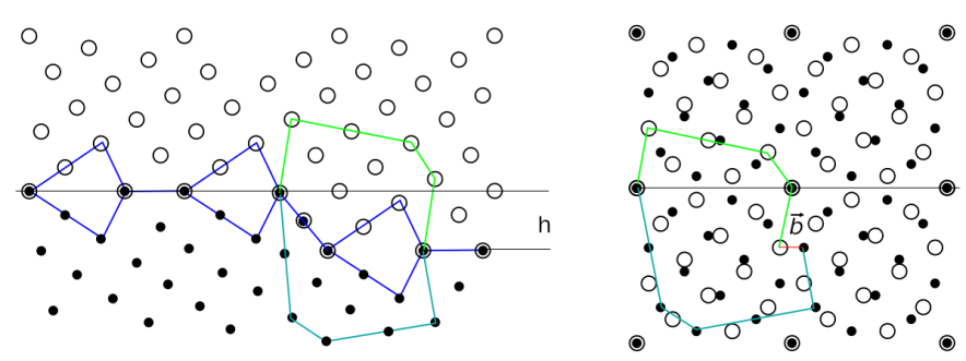
The character and variety of the defects formed at an interface is governed by the extent to which the symmetry of the two crystals are coincident. This feature can be analyzed by looking at the pattern formed when interpenetrating the two crystal lattices and structures (dichromatic pattern and dichromatic complex). The figure below shows the dichromatic pattern formed by two fcc lattices rotated 67.38° around the [001] common axis. This pattern exhibits clearly point group symmetries (four fold symmetry along [001] for example) and antisymmetries ( operation that reverse colors, such as the diagonal mirror for example) and translational symmetries forming a Coincident Cite Lattice (CSL). An ideal bicrystal can be formed by choosing an interface plane, here the (320) plane, and by discarding white lattice site on one side and black ones on the other.

Translational symmetry can be broken considering vectors joining black to white lattice. These vectors formed a sub-lattices called DSC for Displacement Symmetry Conserving 6.

Building a disconnection using the Volterra process is shown below. Consider first a cut surface, here for simplicity, along the (2\bar{3}0) plane (blue dashed line). The cut is then shift by the DSC vector shown by the blue arrow, then glued. The step arises naturally by the fact that the DSC shift changes the coincident positions in the dichromatic pattern. The line defect is along the [001] direction.

To evidence the dislocation character of the defect, the circuit mapping procedure can be applied as shown in the figure below. A closure defect, corresponding to the DSC vector is retrieved by comparing equivalent circuits, both in the defected bicrystal and perfect dichromatic pattern. It can be easily shown that \vec{b}=2/13 a_0 [2\bar{3}0] and h=-5a_0/13

-
J.P. Hirth, J. Phys. Chem. Solids 55 985 (1994) ↩
-
R. C. Pond, in Dislocations in Solids (edited by F. R. N. Nabarro), Vol. 8, p. 1. North-Holland, Amsterdam (1989). ↩
-
We can also call it an interfacial dislocation. ↩
-
Another type of defect arises from crystal presenting screw-rotation symmetry called dispirations ↩
-
Other kind of disconnections can arise when considering broken symmetries due to the existence of glide-mirror of screw rotations (non symmorphic crystals), or shift in the lattice origin that can break the symmetry of the dichromatic pattern. ↩
-
Again, disconnections can arise also if point group symmetries or antisymmetries are broken. ↩